
HTML5 compliant


|
Attention Different browsers interpret web page languages (HTML/ PHP/Javascript/CSS) differently at default. I tuned up this site best for Google Chrome, a most popular browser running on desktops/tablets/ notebooks/mobile phones. Other browsers (Firefox/Edge/IE/ Opera///) might exhibit weird appearance that I do not aim at. |
LSI Products that I was involved in the design
Work categories below are intentionally eliminated from the table as trivial.
(1) Inspection designs at various stages
(2) Customer visit and support
(3) Patents related
(4) Thesis and seminar
(5) Research
(6) Management and presentation
(7) Any other miscellaneous side works
You can make similar tables yourself and recognize what you completed.
People say that "It's easy to say but difficult to do". I say that "It's easy to do but difficult to complete".
(A) NEC, Japan


(1) Custom designed LSIs
| LSI Product |
Year | Architecture Specification |
Logic Design |
Firmware Design |
Breadboard Design |
Breadboard Debug |
Logic Conversion |
Computer Simulation |
Mask Layout Design |
System Evaluation |
LSI Test |
| 31 | 1971 | customer | customer | hardwired | customer | customer | 100% | 100% | contractor | 0% | 0% |
| 32 | 1971 | customer | customer | hardwired | customer | customer | 100% | 100% | contractor | 0% | 0% |
| 33 | 1971 | customer | customer | hardwired | customer | customer | 100% | 100% | contractor | 0% | 0% |
| XX | 1971 | customer | customer | hardwired | customer | customer | 100% | 0% | contractor | abandoned | abandoned |
[31, 32, 33]
Mr.Tomoyo Ichikawa of Eiko Business Machine, Inc. designed the original
logic for 8 digits desk-top calculator with Eiko proprietary printer
and divided the entire logic into five LSIs nick-named 31, 32, 33,
34, and 35. Soon after I started working at NEC in June, 1971, I
took charge of 31, 32, and 33 that functioned as Central Processing
Unit, data memory, timing generator, and so forth. I completed the
logic conversion from the original logic schematics given by Eiko
Business Machine to NEC logic modules (blocks) to ease the mask
layout utilizing building blocks scheme as well as the computer
simulation. 34 and 35 were Printer Control Unit and handled by Mr.
Shimizu of NEC. Mr. Shimizu took over system evaluation and LSI test
for all the five LSIs later on.
The computer simulation for LSI was an emerging technology intensively
using main frame at that time. The net list and simulation vectors
were punched on IBM 80 column punch cards line by line.
[XX]
XX was a single-chip 8 digits desk-top calculator LSI designed by Tokyo
Electronic Application Laboratory (President: Hitoshi Kodaira; 東京電子応用技術研究所) based on development request from
NEC. NEC did not have sufficient ability to design desk-top
calculator LSI at that moment. Although I was not a person in charge
of the project, I was requested to complete the logic conversion
because only a limited number of LSI designers was able to do the
work. Because NEC strongly promoted the XX project, a most
experienced contractor was assigned for the mask layout as well.
However, the die size after the actual mask layout had become larger
than 5mm x 5mm due to a lot of internal wire connections derived from
the hard-wired random logic design. At that time, it was common
knowledge that the yield became zero (no good die per silicon wafer)
if the die size became beyond 5mm x 5mm.
At the next stage, I was requested to try to divide the entire logic
into two LSIs (this means that it is not a single-chip LSI). My
conclusion was “Unrealistic and Impossible” because the
number of LSI pins easily went beyond 28 pins due to a lot of
interconnects. The maximum number of LSI pins available was 28 at
that time because of the constraint of LSI packaging technology.
Consequently,
the project XX was eventually abandoned.
Mr. Atsuyoshi Ouchi, a manager of NEC Integrated Circuit division,
decided to pay the compensation for the development to TEAL although NEC did not make anything and any profit from XX. Mr.
Kurokawa, a section manager, applauded the reaction saying “It
is good for future”.
This event triggered two big projects for developing 8 digits single-chip
desk-top calculator LSI (µPD271) and 12 digits multiple-chip desk-top calculator LSI chip-set
(µPD281; program ROM etc., µPD282; Register files + ALU (Arithmetic Logic Unit),
µPD261; Segment decoder, µPD262; Timing counter, µPD264; External memory
register)
to be designed by NEC's own efforts.
Mr. Tomihiro Matsumura, a manager of second circuit technology
department (第二回路技術部), promptly organized the LSI development projects in March,
1972, and held the kick-off meeting. Although I did not know why
this happened, probably unfortunately, I had sat down a seat just in
front of Mr. Matsumura of a square desk for 5 x 6 people (Yamamoto,
Shiraishi, Matsumura, Takashima, Kurokawa vs. Tanaka, Ariga, Takai,
Oguchi, Maehashi, Oura). As soon as I sat down, Mr. Matsumura
immediately started arguing me saying, “Oguchi-kun, although
you may be a rookie......” He disputed my reactions and
resolutions concerning aforementioned XX LSI development. He seemed
not to know the whole course of events that most people sitting there
knew well. I gazed at Mr. Takashima sitting left beside Mr.
Matsumura considering that he tried to evade his responsibility (this
was the first job for him just after appointed to a supervisor.) and
transferred it all to me. Because I believed that I did the best and
the original design had fatal weak point of hard-wired design
approach (Moreover, this is not my own design!), I sat still thinking
that “This is My Way”.
Tomorrow morning, Mr. Takai and Ariga who were actually people in charge of XX
product came to me and told that “Just leave it”. Mr.
Shiraishi, a manager of device design section, also came and told
that “After you left, I clearly defended you with the truth. I
usually say what I want to say.” This was his nature derived
from his origin of Kyusyu island that most Japanese did not have.
(2) NEC originally designed LSIs
(not based upon reverse engineering as well as customer's design)
Excerpt from Manuscript of JIEC seminar (page 3)
LSI Device seminar
| LSI Product |
Year | Architecture Specification |
Logic Design |
Firmware Design |
Breadboard Design |
Breadboard Debug |
Computer Simulation |
Mask Layout Design |
System Evaluation |
LSI Test |
| µPD282Updated on 6/14/25 |
1972 | 30% | 100% | hardwired | 50% | 10% | 100% | 100% | 100% | 100% |
| µPD940Updated on 5/26/25 |
1973 | 100%Updated on 6/15/25 |
100% | 50% | 20% | 0% | 100% | 100% | 100% | 100% |
| µPD941 | 1974 | derivative | derivative | 100% | derivative | 100% | 100% | derivative | 100% | 100% |
| µPD942 | 1974 | derivative | derivative | 100% | derivative | 100% | 100% | derivative | 100% | 100% |
| µPD943 | 1974 | derivative | derivative | 100% | derivative | 100% | 100% | derivative | 100% | 100% |
| µPD947Updated on 6/15/25 |
1975 | 0% | 0% | 0% | 0% | 0% | 0% | 0% | 0% | 100% |
| µPD1201 | 1975 | 100% | 100% | 50% | 0% | 0% | 100% | 100% | 100% | 100% |
| µPD1202 | 1975 | derivative | derivative | 100% | derivative | 100% | 100% | derivative | 100% | 100% |
| µPD1203 | 1976 | derivative | derivative | 100% | derivative | 100% | 100% | derivative | 100% | 100% |
| µPD1205Updated on 12/30/25 |
1976 | 100%Updated on 6/15/25 |
100% | 80% | 50% | 100% | 0% | 0% | 0% | 0% |
| µPD777 | 1977 | 50%Updated on 12/13/25 |
90% | 20% | 90%Updated on 6/14/25 |
0% | 0% | 100% | 0% | 0% |
| µPD7220Updated on 6/15/25 |
1981 | 100% | 100% | hardwired | 100%Updated on 9/13/25 |
100% | 0% | 5% | 100% | 0% |
| µPD7220A | 1983Updated on 6/15/25 |
derivative | 100% | hardwired | 100% | 100% | 0% | 50% | 100% | 0% |
| µPD72120 | 1987Updated on 6/15/25 |
100%Updated on 6/15/25 |
0% | 0% | 0% | 100%Updated on 6/15/25 |
0% | 0% | 100% | 0% |
[µPD282]
I fully took charge of µPD282, a CPU with memory LSI for 12 digits 1 memory desk-top calculator.
The logic design completed less than one year later I joined NEC in 1971. µPD282 along with µPD281 is the first logic LSI
that NEC originally designed from scratch.
The development project was initiated by powerful direction of Mr.
Tomihiro Matsumura, a department manager, due to the abortion of
single-chip LSI design (XX as mentioned above) for 8 digit calculator
that NEC requested to external independent design house.
I
was so lucky because I was able to build broad LSI design expertise
through the actual µPD282 design in very early stage of my engineering life.
Functions
- 4 x 64 bits (for 12 digits BCD data with one overflow digit + decimal point
BCD data digit + control digit + sign digit) ratio-less shift registers
- 1 x serial BCD full adder/subtractor with carry calculation
- Instruction decoder
- Judge output and ROM code inputs to/from µPD281
- Data & timing outputs to µPD261 segment decoder
- Timing input/output to/from µPD262 digit timing generator
- Data output & input to/from µPD264 extended memory
- Display data outputs to 8 segment fluorescent digit display tubes
Process & Design
10μ P channel metal gate E/E MOS using building block mask
layout, VGG = -24V, VDD = -12V, GND = 0V, Two phase clocks (/φ1, /φ2),
Capacitive dynamic shift registers and transmission gate design
System structure
The 12 digits 1 memory desk-top calculator system consist of a µPD281
(ROM + address sequencer + keyboard decoder; 24 pin ceramic DIP LSI),
a µPD282 (CPU + memory; 28 pin ceramic DIP LSI), a µPD261 (8 segment decoder; 20 pin plastic DIP MSI),
a µPD262 (digit timing generator; 20 pin plastic DIP SSI). µPD264
(extended memory; 20 pin plastic DIP MSI) can be attached to increase
the number of data memories.
Abbreviations
CPU (Central Processing Unit), BCD (Binary-Coded Decimal), ROM (Read-Only Memory), DIP
(Dual-Inline Package), E/E (Enhancement mode for load MOS
transistor/Enhancement mode for gate MOS transistor), MOS (Metal
Oxide Semiconductor), VGG (Voltage supplied to Gate of load MOS
transistor), VDD (Voltage supplied to Drain of load MOS transistor),
GND (Ground voltage), LSI (Large-Scale Integration), MSI
(Medium-Scale Integration), SSI (Small-Scale Integration)
Although everybody expected that the mask-layout of the µPD282
is done by a contractor as usual, I started mask-layout design as
soon as I completed logic design and computer simulation. Mr.
Matsumura came to me and told mischievously with smile, “You
are doing the mask-layout with strong guts, aren't you?”
I experienced work through the night three times for breadboard debug
and x200 stabylen film cut mask base inspection to be done before ordering
physical photo masks.
Mr. Oura taught me how to handle LSI testers, ASR33 teletypewriter, paper
tape, and how to modify the paper tape hole positions by using tape puncher.
update in progress
[µPD940 - µPD943]
update in progress
[µPD1201 - µPD1203]
update in progress
[µPD1205]
update in progress
[µPD777]
update in progress
(B) Chips and Technologies, USA
[82C455 - 82C457]
(C) ASCII of America, USA
[DA7290 - HD814102]
(D) Auctor Corporation, USA
[YY]
(E) SanDisk, USA
[Bishamon] Micrograph Related About Litigation between Western Digital & Toshiba
Excerpt from manuscript of JIEC seminar (page 7)
Application exapmle :
Epoch Cassette VisionCartridgeUpdated on
6/14/25
Epoch Cassette VisionAnatomyUpdated on
6/14/25
On-chip ROM Dump Related
- System Design of ROM dumpUpdated on
6/14/25
- Dump Pattern Creation
- Dump source pattern (PA.txt)Updated on
6/14/25
- Source code of "rom_dump.cpp"Updated on
6/14/25
- Dump Analysis
- Source code of "dump_analysis.cpp"Updated on
6/14/25
- Dump Result of µPD777 004 Big Sports 12
- Program ROM
- Pattern ROM
- Dump Result of µPD778 Baseball
- Program ROM
- Pattern ROM
- Dump Result of µPD774 Battle Vader
- Program ROM
- Pattern ROM
- Dump Result of µPD777 005 Yosaku
- Program ROM
- Pattern ROM
- Dump Result of µPD777 007 Galaxian
- Program ROM
- Pattern ROM
- Dump Result of µPD777 008 Pakpak Monster
- Program ROM
- Pattern ROM
- Dump Result of µPD777 009 Monster Mansion
- Program ROM
- Pattern ROM
- Dump Result of µPD777 010 Astro Command
- Program ROM
- Pattern ROM
- Datasheets
- 27SF512 (64KB x 8 EPROM)Updated on
5/28/26
- CXK58256 (32KB x SRAM)Updated on
5/28/26
777 to YUV Related
- System Design of 777 to YUVUpdated on
6/14/25
- Video Files
- µPD777 005 Yosaku
- µPD778 Baseball
- µPD777 007 Galaxian
- µPD777 Big Sports 12
- µPD774 Battle Vader
- µPD777 008 Pakpak Monster
- µPD777 009 Monster Mansion
- µPD777 010 Astro Command
- Datasheets
- BA7230 (NTSC Color TV Signal Encoder)Updated on
5/28/26
- THS7374 (Quad SDTV Video Amplifiers with Low-Pass Filter)Updated on
5/28/26
- LM319 (Dual Comparators)Updated on
5/28/26
- LM6172 (Dual Amplifiers)Updated on
5/28/26
NTSC TV Video (RF) Modulator ICs
- NEC µPC626C for µPD777C
(See page 6 of "777 Design Note.pdfUpdated on
12/13/25")
- NS LM1889 (µPC626C compatible)
[µPD7220 - µPD7220A]
update in progress
Tandy Radio Shack TRS-80 (8 bit personal computer released in 1977) Related
- TRS-80 Schematics etc.Updated on
9/13/25
- WD FD1771 Floppy Disk Controller
[µPD72120]
update in progress
Remarks :
(A) The trial productions were always handled by device design team using photo masks I ordered
to Toppan Printing or Dai Nippon Printing as a result of mask layout design.
(B) LSI testers I used for trial production and evaluation were MH-134 (Minato Tsushinki),
MH-152 (Ando Electric), and MH-200 (Ando Electric).
(1) For wafer check (P/W test), I ordered probe cards based upon pin connection and bonding
pads' position information.
(2) For screening test (選別) and warehousing test (入庫), I ordered DUT (Device Under Test) boards.
(3) For BT (Bias Temperature) test, I ordered BT boards.
(4) For system level test (実装), I made manually-driven system level testers and test programs for
automatic system level testers designed as a result of co-operation
with automation department, later on (applied to µPD282 to µPD1205, 1972 - 1976).

LSI
ProductYear
Architecture
SpecificationLogic
DesignFirmware
DesignBreadboard
DesignBreadboard
DebugComputer
SimulationMask Layout
DesignSystem
EvaluationLSI
Test
82C455
1988
100%
100%
hardwired
none
none
100%
gate array
(Toshiba/
LSI Logic)100%
100%
82C456
1989
100%
100%
hardwired
none
none
100%
gate array
(Toshiba)100%
100%
82C457
1990
100%
100%
hardwired
none
none
100%
gate array
(Toshiba)100%Updated on
6/14/25100%
I designed these three IBM VGA compatible flat panel graphics LSIs under joint
development program between ASCII and Chips and Technologies exchanging the
Letter of Intent.
Development historyUpdated on
6/14/25 of 82C455, 82C456, and 82C457
Probing VGA/SVGA/XGAUpdated on
6/14/25 video signals
Gate Array specification
- TC110G Toshiba CMOS Gate Array
Netlist related information
- FRC (Frame Rate Control) Scheme EvaluationUpdated on
6/14/25 8086 Assembly source code
- TC110G MacrocellsUpdated on
6/14/25 Implemented on 82C457
82C457 Application Examples
- Dolch Color flat panel portable PC
- Alcon Surgical equipment Series 20000
- 82C9001A Data sheet introduces 82C457
Datasheet of companion chips
- 82C460 Flat Panel Color Palette
- 82C401 Flat Panel/CRT Clock Synthesizer
- 82C411 Flat Panel Color Palette/DAC
Flat panel specification (Extracted)
- Sharp DD (Dual panel Double drive) STN (Super Twisted Nematic) panel
- Sharp 512 Color TFT (Thin Film Transistor) panel
US patents applied at Chips and Technologies Inc.
- Go to here. I am ranked as a #4 inventor.

LSI
ProductYear
Architecture
SpecificationLogic
DesignFirmware
DesignBreadboard
DesignBreadboard
DebugComputer
SimulationMask Layout
DesignSystem
EvaluationLSI
Test
DA7290
1993
0%
0%
hardwired
none
none
0%
gate array
(VLSI Technology)100%
gate array
HD814102
1994
2%Updated on
6/22/252%
hardwired
none
none
0%
gate arrayUpdated on
6/22/25
(Hitachi)100%
gate array
- MPEG1 Audio Specification
MPEG1 audio compression scheme has been using on Movie DVD/Bluray and MP3 (Originaly named from MPEG1 audio Layer 3) audio players.
MPEG skipped MPEG3 and now MPEG4 (MP4; Video and audio compression).
update in progress
LSI
ProductYear
Architecture
SpecificationLogic
DesignFirmware
DesignBreadboard
DesignBreadboard
DebugComputer
SimulationMask Layout
DesignSystem
EvaluationLSI
Test
YY
1996
100%
100%Updated on
6/16/25100%
50%
80%
80%
gate array
abandoned
abandoned
- Flash memory controller LSI design work reportUpdated on
10/12/25 written by Ramesh Achalu.

LSI
ProductYear
Architecture
SpecificationLogic
DesignFirmware
DesignBreadboard
DesignBreadboard
DebugComputer
SimulationMask Layout
DesignSystem
EvaluationLSI
Test
Bishamon
2000
100%
100%
100%
80%
100%
100%
gate array
abandoned
abandoned
update in progress
History of LSI Design Methodology
- Transition of LSI Design
- Breadboard Design History
Silicon Valley Maps
- 1945 Vintage
Woodside, Atherton, Menlo Park, Palo Alto, Mountain View, Los Altos, Sunnyvale
- 1975 Vintage
Mountain View, Los Altos, Sunnyvale, Cupertino, Saratoga, Monte Sereno
- Map ComparisonEvergreen, San Jose, CA (1975 vs. 2023)
- 1981
- 1982
(Fairchild, NEC Electronics USA, Varian,
Apple, Zilog, NEC America,
Fujitsu Microelectronics, Advanced Micro Devices,
Megatest, Atari, Monolithic Memories, Seeq, LSI Logic,
Dolch, Weitek, Ramtek, IBM, Paul
Masson Cellars,,,)
- 1983
- 1987
(Chips and Technologies,
Mentor Graphics, Linear Technology, VLSI Technology, Sun Microsystems, Silicon
Graphics, Toshiba America, Intel,
Hewlett Packard,,,)
- 1991
(Oracle, Seagate, Cirrus Logic, KLA, Amdahl, Siemens, Teledyne
Components, National Semiconductor, Televideo, IKOS,
Motorola, Tandem, ACC Micro,
Symantec, Raster Ops, Borland, Xilinx,,,)
- 2001
- 2005
(Info World, Hitachi, EE Times, SAP,
San Disk, VeriSign, Altera, Texas
Instruments, Yamaichi Electronics, Teradyne, ST Microelectronics,
Sanyo, Infineon, Vishay, nVidia, Mitsui Comtek,
Arm,,,)
- 2013
- 2018
Have worked @,
Have visited to
- Die Photo Synthesis by Hugin
- Die Photo Synthesis by Hugin (Scanned Map)
- Decapsulation of Ceramic DIP
- Decapsulation of Plastic DIP
- Epoxy Removal by Ultrasonic
- Zooming up Die Micrograph on PDF File
I am introducing total 25 die micrographs I made.
When zooming die micrograph using a smart phone or tablet, you possibly experience limited maximum available zoom factor (up to 2x), slow zooming speed, and sometimes freeze because of the factors such as slow CPU, insufficient main memory capacity, and simplified PDF viewer installed.
I recommend using a desk-top PC with large monitor TV (40”), fast CPU (i7), big capacity of main memory (32/16 GB), and fast GPU (8 GB) if possible.
Design
companyManufacturing
companyProduct
NameFunction
NEC
µPD282D
12 Digit Desk-top Calculator (ALU, Registers, etc. ) <Tetsuji Oguchi>
µPD941C
Single-chip 8 Digit 0 memory Desk-top Calculator <Tetsuji Oguchi>
µPD946C
Single-chip 8 Digit 1 memory Desk-top Calculator
µPD1201C
Single-chip 12 Digit 1 memory Desk-top Calculator with Printer Control <Tetsuji Oguchi>
µPD777D
Single-chip Television Game Processor <Tetsuji Oguchi & Toshio Oura>
µPD777C
µPD7220AD
Graphics Display Controller (GDC) <Tetsuji Oguchi>
NEC
Intel
iD82720
Graphics Display Controller (GDC)
- License manufacturing (Second source) of µPD7220
NEC
µPD72120L
Advanced Graphics Display Controller (AGDC) <Tetsuji Oguchi, et al.>
µPD765C
Floppy Disk Controller {NEC Fuchu Peripheral Equipment Division}
Microprocessor version of WD LD1771
µPD7720AD
Signal Processor {NEC Central Research}
µPD277
Single-chip 8 Digit 1 memory Desk-top Calculator <Toshio Oura>
Casio
NEC
µPD977
Single-chip 8 Digit 1 memory Desk-top Calculator
µPD871B
Digital watch
µPD873G
Intel
8080A
8 bit Microprocessor
8085A
8 bit Microprocessor
iD8086
16 bit Microprocessor
Intel
NEC
µPD8086D
16 bit Microprocessor
- Reverse engineering of iD8086
Oki
80C86A
16 bit Microprocessor
- License manufacturing (Second source) of iD8086
Zilog
84C00
8 bit Microprocessor (Z80)
Nintendo
Ricoh
RP2C02
Television Game Processor (Family Computer with RP2A03)
Motorola
RP2A03
8 bit Microprocessor
- Reverse engineering of Motorola 6800
Motorola
68000
16 bit Microprocessor (Apple Macintosh)
TI
TMS9918A
Television Game Processor (Multiple chips)
{}; Architectural design by
<>; Architectural & Logic design by
Enginnering Analysis Report
- SC 179 LSI (Scientific Calculator LSI; 3/4/1974)
- SC 978 LSI (Scientific Calculator LSI; 1/21/1975)
Approximations for Digital ComputersUpdated on
6/19/25 by Cecil Hastings Jr.
- HP Model 65Updated on
12/23/25 (Scientific Calculator with programming function by magnetic tape; 3/10/1975)
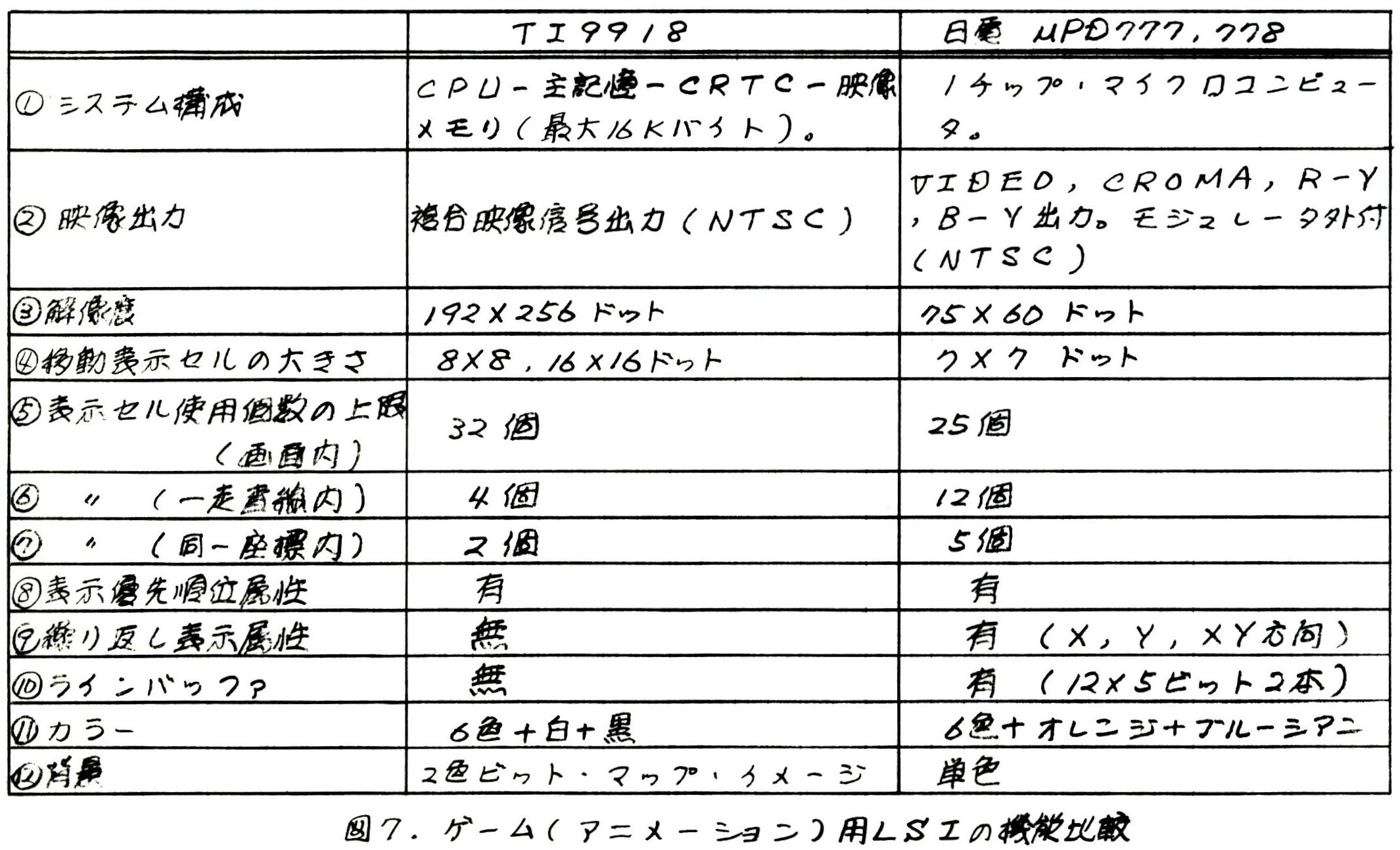
Video Game LSIs
VDP (Video Display Processor) Analysis (contributed by Mr. Masao Hirasawa, ex-NEC; 9/22/1983)
- NEC
µPD777 (Epoch Cassette Vision etc.)
- Texas Instrument
TMS9918 (Sega SC-3000 etc.)
- Ricoh
RP2C02
(First generation of Nintendo's Family Computer)
ESP32 Related
Datasheets
- ESPRESSIF ESP32 (32 bit Dual Core CPU with various peripherals)Updated on
5/12/26
- ESP32-S3-DevKitC-1Updated on
6/28/26
- ESP32-S3-DevKitC-1 SchematicsUpdated on
5/13/26
- ESP32 I2CUpdated on
5/21/26
- ESP32 I2SUpdated on
5/21/26
- ESP32 SPIUpdated on
5/21/26
- Hitachi HD44780 (40 x 16 B/W LCD Driver/Controller)Updated on
3/11/26
- ILITEK ILI9341 (240 x 320 Color LCD Driver with Graphics RAM)Updated on
2/25/26
- MAXIM MAX98357A (Class D Audio Amplifier)Updated on
2/25/26
- NXP PCF8574 (I2C to Parallel)Updated on
2/20/26
- NXP XPT2046 (Touch Screen Controller)Updated on
2/24/26
Specifications
- I2CUpdated on
2/24/26
- I2SUpdated on
2/26/26
- SPIUpdated on
2/26/26
Audio Video Processing Related
-
Nvidia Graphics Card Installation
-
Heaven UNIGINE benchmark result
-
Final Fantasy benchmark result
-
Topaz Photo AI photo image improvement result
Nintendo's Family Computer (HVC-001)
I have visited Nintendo in 3/1983. It was normal that at least five people
attended when I visited various customers. Therefore, it was so special
for me that only one person attended the meeting held at Nintendo. His name was Mr.
Tsutomu Yamao (Probably, he was involved in HVC-001 development with Mr.
Masayuki Uemura as a deputy manager).
We talked in a room where three arcade game machines were
displayed. After the technical talk completed, he brought us to bigger room
next door filled with
so many arcade game machines. Just before we were leaving, he disclosed that "Nintendo will
release a new game machine for home next month." The product was the epoch-making "Family
Computer".
As soon as it was actually released in 7/1983, he gave me three
Family Computers and six game cartridges with different title.
Over five
years had passed since NEC µPD777/µPD778 (7 bit single-chip microcomputer for
game application adopted by Epoch later on) were released in 1978.
- Family Computer
- Super Mario Music
- Short video of Mr. Masayuki Uemura
FPGA
- FPGA Board
- VGA Color Bars
Users Manuals and Design Manuals
- Users Manual NEC µPD7220AUpdated on
6/15/25
- Users Manual NEC µPD72120Updated on
6/15/25
- Design Manual NEC µPD7720
- Datasheet Chips and Technologies 82C455
- Datasheet Chips and Technologies 82C456
- Datasheet Chips and Technologies 82C457
- Datasheet NEC 41256 Dual Port 256k bit DRAM for Graphics Application
Personal Computer Schematics
- NEC TK-80 (8 bit Training kit)Updated on
6/14/25
Datasheets of major LSIs installed on TK-80
- 8080Updated on
2/23/25 8 bit Central Processing Unit
- 8212Updated on
2/23/25 8 bit Input Output Port
- 8224Updated on
2/23/25 Clock Generator
- 8228Updated on
2/23/25 Bus Controller
- 454Updated on
2/23/25 256 x 8 EEPROM
- 5101Updated on
2/23/25 256 x 4 SRAM
- Tandy Radio Shack TRS-80 (8 bit personal computer)Updated on
9/13/25
Datasheets of major LSIs installed on TRS-80
- Zilog Z80 8 bit Central Processing Unit
- WD FD1771 Floppy Disk Controller
- NEC PC8001 (8 bit personal computer)
Datasheets of major LSIs installed on PC8001
- 780 8 bit Central Processing Unit (Reverse engineering of
Zilog Z80)
- 3301 Cathode Ray Tube Controller (Reverse engineering of
Intel 8275 with
row buffer and FIFO expansion to make 7 bits coding to 8 bits)
- 8257 Direct Memory Access Controller (Reverse engineering of Intel 8257)
- NEC PC9801 (16 bit personal computer)
Datasheets of major LSIs installed on PC9801
- 8086 16 bit Central Processing Unit (Reverse engineering of Intel 8086)
- 8087 16 bit Mass co-Processor (Reverse engineering of Intel 8087 by NEC failed due to skill limit there.)
- 7220Updated on
6/15/25 Graphics Display Controller (Intel obtained license manufacturing;
82720) x 2
- 765 Floppy Disk Controller (Microprocessor version of
WD FD1771. See NEC 8 inch floppy disk drive
FD1165 datasheet.)
- 8237 Direct Memory Access Controller (Reverse engineering of Intel 8237)
- 8251 Universal Synchronous/Asynchronous Receiver/Transmitter x 3 (Reverse engineering of Intel 8251. 7201, reverse engineering of
Z80 SIO, was not adopted.)
- 8253 Interval Timer (Reverse engineering of Intel 8253)
- 8259 Interrupt Controller (Reverse engineering of Intel 8259) x 2
- 7210 General Purpose Interface Bus Controller
- 8255 Programmable Inputs/Outputs (Reverse engineering of Intel 8255) x 4
- 1990 Callendar & Clock
- 8284 Clock Generator (Reverse engineering of Intel 8284)
- 8288 Bus Controller (Reverse engineering of Intel 8288)
- 4164 64k x 1 Dynamic Random Access Memory x 16
- 23128 16k x 8 Read-Only Memory x (16 + 10)
- 2764 8k x 8 Electrically Programmable Read-Only Memory
- 4016 2k x 8 Static Random Access Memory x 3
- 416 16k x 1 Dynamic Random Access Memory x 48
NEC was good at reverse engineering (Takeoff, 物まね) of LSIs originally designed by foreign companies such as Fairchild, Texas Instrument, Intel, and Zilog.
Most LSIs which was said to be designed by NEC IC division were originated from architectural designs by NEC in-house divisions such as Fuchu, Central research, and Abiko
except desk-top calculator LSIs, 4 bit and 8 bit single-chip microprocessors, and graphics LSIs such as µPD7220/72120.
Such takeoff was not sustainable, did not spawn creativity and true ability, and made siege mentality eventually.
Joint Venture of SanDisk and Toshiba
SanDisk acquired by Western Digital and Toshiba
mutually established joint venture concerning NAND flash memory development
& manufacturing at Yokkaichi, Mie, Japan in 2000.
For last 17 years, the two companies have been investing a lot, $XY billion, in proportion to
Toshiba (51%) and SanDisk (49%) beyond five generations of factory
expansion, etc..
As a result of the joint development, San Disk and Toshiba co-authored papers (theses) for prestigious IEEE (Institute of
Electrical and Electronics Engineers) ISSCC (International Solid State
Circuit Conference) and 13 theses were accepted (See “ISSCC
Papers Co-aurthored.pdf”).
SanDisk and Toshiba co-assigned US
patents and 123 patents were registered (See “US
Patents Co-assigned.pdf”).
Western Digital's Concerns
Based upon the long term successful cooperation,
Western Digital expressed help bailing out Toshiba facing with fatal
financial problem (See “WD Willing to Help Toshiba.pdf”),
4/25/2017.
Western Digital CEO Steve Milligan kindly stated concerning
Toshiba problem at WD 2017 third fiscal quarter conference call (Listen to “Milligan
Comment about Toshiba” and read ”Dictation
of Milligan Comment”), 4/27/2017.
Sanjay Mehrotora & Khandker Quader
The joint venture was initiated by Sanjay Mehrotora (Vice president R&D, in
those days) who also requested SanDisk acquisition to Western Digital in
August 2015 as President & CEO of SanDisk.
Khandker Quader led flash memory design cooperating with Toshiba.
The two people already left SanDisk (See “Sanjay
& Khandker.pdf”)
Khandker became President & CEO of SK Hynix
Memory Solutions which is US subsidiary of SK Hynix in June, 2013.
Lawsuit against SK Hynix was filed by SanDisk and
Toshiba in March, 2014 (See “Lawsuit against SK
Hynix.pdf”).
Khandker left SK Hynix Memory Solutions in June,
2014, during the lawsuit.
Sanjay became board member of Western Digital for a while. Then, Sanjay became President & CEO of Micron
Technology in May, 2017.
Micron Technology acquired Lexar Media, one of
competitors of SanDisk flash memory business, in 2006.
Micron Technology fully acquired Elpida Memory,
a Japanese sole DRAM manufacturer merged in NEC (Nippon Electric Company)
and Hitachi, in 2013.
Settlement Announcement
Western Digital CEO Steve Milligan announced the
eventual achievement of the settlement.
(Listen to “Milligan
Announcement about Toshiba” and read ”Dictation
of Milligan Announcement”), 12/12/2017.
My Way of Engineering Life
I keenly feel with the fact that this
song (My Way) exactly expresses my way of engineering life.
My Way
And now, the end is near.
And so I face the final curtain.
My friend, I'll say it clear.
I'll
state my case of which I'm certain.
I've lived a life that's full.
I've traveled each and every highway.
And more, much more than this,
I
did it my way.
Regrets, I've had a few.
But then again, too few to
mention.
I did what I had to do,
And saw it through without exemption.
I planned each charted course.
Each careful step along the byway.
And more, much more than this,
I did it my way.
Yes, there were
times, I'm sure you knew
When I bit off more than I could chew.
But
through it all, when there was doubt,
I ate it up and spit it out.
I
faced it all and I stood tall,
And did it my way.
I've loved, I've
laughed and cried.
I've had my fill, my share of losing.
And now, as
tears subside,
I find it all so amusing.
To think I did all that,
And may I say - not in a shy way?
"Oh no, oh no not me,
I did it my
way".
For what is a man, what has he got?
If not himself, then he
has naught.
To say the things he truly feels,
And not the words of one
who kneels.
The record shows I took the blows,
And did it my way!